
Patch inductance and current convert electrical energy, store it, and then release it, which is why capacitors discharge. Resistance consumes electrical energy and converts it into heat energy, which cannot be released again. Capacitors convert electrical energy into potential energy, and patch inductors convert electrical energy into magnetic energy. Potential energy can discharge electricity, and magnetic energy can generate electricity, while heat energy cannot be converted back through resistance. So the resistance is consuming energy. Both inductance and capacitance act as obstacles to current. Inductance is used to maintain current, and inductance is used to direct current to prevent AC, because it is meaningless for direct current to pass through the inductance, because the magnetic field does not change. The capacitor is to maintain the voltage, is the current through the alternating current, because the capacitor in the DC circuit is equivalent to open, capacitor is to maintain the voltage.
When the inductor is energized, the self-induced electromotive force u=dψ/dt=L? Di /dt. According to Lenz's law: when I increases, the direction of the induced current is opposite to that of I. When the inductance coil is just energized, the current changes rapidly and the induced current is very large, which is superimposed with the original current, so that the current in the coil can only increase from 0 until the current changes to 0, and then the current in the coil can reach the maximum. So, the inductor coil has a delay effect. The inductor can realize the filtering function by using its on-direct-resistance-to-traffic characteristics. And can be combined with the capacitor into a different filter circuit. Figuratively speaking, Filtering is the blocking of alternating current signals like waves; Therefore, The ac component is the object of filtering; And filtering ac components; Pure dc component can be obtained; Patch inductor at the power supply end; After rectifying the circuit, the filter function is generally realized.
Inductance is a property of a closed circuit, that is, when the current through the closed circuit changes, there will be an electromotive force to resist the current change. This inductance, called self-induction, is a property of the closed loop itself. If a change in current in one closed circuit causes an electromotive force to be induced in another closed circuit, the inductance is called mutual inductance. When two inductance coils are close to each other, the magnetic field change of one inductance coil will affect the other inductance coil, and this effect is mutual inductance. The mutual inductance depends on the degree of coupling between the self-inductance of the inductance coil and the two inductance coils. The element made by this principle is called transformer.
Patch inductor is an electromagnetic induction element wound with insulated wire. It is a common inductance element. The role of the patch inductor: through DC resistance AC this is a simple way of saying that the AC signal is isolated, filtered or resonated with capacitors, resistors, etc. The role of tuning and frequency selection inductor: the LC tuning circuit can be composed of inductive coil and capacitor in parallel. Any current in the patch inductor in the circuit generates a magnetic field, the flux of which acts on the circuit.
As the current through the patch inductor changes, the DC voltage potential generated in the patch inductor will prevent the current from changing. When the current passing through the inductance coil increases, the inductance coil generates the self-induced electromotive force and electricity. When the current passing through the inductance coil decreases, the self-induced electromotive force is in the same direction as the current, preventing the current from decreasing and releasing stored energy to compensate for the decrease in current. The current direction is opposite to prevent the increase of current, while part of the electric energy into a magnetic field can be stored in the inductor; Therefore, after the inductance filtering, not only the load current and voltage pulsation is reduced, the waveform becomes smooth, and the rectifier diode conduction angle increases.
SMD inductor with general SMD inductance shielding, general SMT inductance in the circuit is without blocking, use up in the circuit inductance is less than the desired effect, shielding SMT inductance can block out some of the current in the circuit is not stability, good have the effect of blocking, shielding inductive complete metal shield will positively charged conductor surrounded by On the inside of the shield body, the negative charge equal to that of the charged conductor will be induced, and the positive charge equal to that of the charged conductor will appear on the outside. If the metal shield body is grounded, the positive charge on the outside will flow into the earth, and there will be no electric field on the outside, that is, the electric field of the positive conductor will be shielded in the metal shield body.
The shielding inductance also plays a coupling role in the circuit. In order to reduce the coupling interference voltage of the sensitive circuit caused by alternating electric field, the shielding metal body with good conductivity can be set between the interference source and the sensitive circuit, and the metal shielding body can be grounded. The coupling interference voltage of alternating electric field to sensitive circuit depends on the product of alternating electric field voltage coupling capacitance and grounding resistance of metal shield. As long as the metal shield is well grounded, the coupling interference voltage of the alternating electric field to the sensitive circuit can be minimized. The electric field shielding is mainly reflected, so the thickness of the shielding body need not be too large, and the structural strength is the main factor to consider.
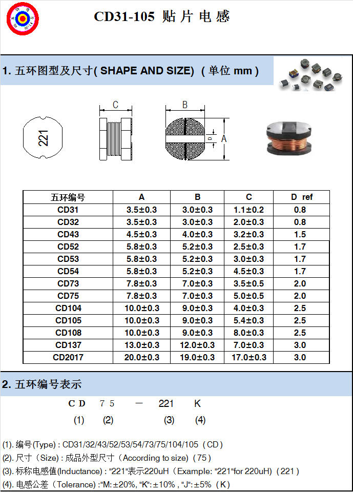
CD31 series of characteristics
|
The five rings number |
L |
TESTING |
DC |
RATED DC |
|
FREQ. |
RESISTANCE |
CURRENT |
||
|
uH |
(KHz). |
(Ω) MAX. |
A MAX |
|
|
CD31-2R2M |
2.2 |
100KHZ |
0.24 |
1.20 |
|
CD31-3R3M |
3.3 |
100KHZ |
0.27 |
1.08 |
|
CD31-4R7M |
4.7 |
100KHZ |
0.30 |
1.00 |
|
CD31-6R8M |
6.8 |
100KHZ |
0.47 |
0.80 |
|
CD31-8R2M |
8.2 |
100KHZ |
0.52 |
0.76 |
|
CD31-100M |
10.0 |
100KHZ |
0.55 |
0.70 |
|
CD31-120M |
12.0 |
100KHZ |
0.75 |
0.60 |
|
CD31-150M |
15.0 |
100KHZ |
0.91 |
0.50 |
|
CD31-220M |
22.0 |
100KHZ |
1.20 |
0.40 |
|
CD31-270M |
27.0 |
100KHZ |
1.50 |
0.36 |
CD32 series of characteristics
|
The five rings number |
L |
TESTING |
DC |
RATED DC |
|
FREQ. |
RESISTANCE |
CURRENT |
||
|
uH |
(KHz). |
(Ω) MAX. |
A MAX |
|
|
CD32-100K |
10 |
100 |
0.23 |
0.760 |
|
CD32-120K |
12 |
100 |
0.27 |
0.685 |
|
CD32-150K |
15 |
100 |
0.31 |
0.635 |
|
CD32-180K |
18 |
100 |
0.41 |
0.525 |
|
CD32-220K |
22 |
100 |
0.47 |
0.500 |
|
CD32-270K |
27 |
100 |
0.66 |
0.405 |
|
CD32-330K |
33 |
100 |
0.76 |
0.380 |
|
CD32-390K |
39 |
100 |
0.85 |
0.355 |
|
CD32-470K |
47 |
100 |
0.97 |
0.330 |
|
CD32-560K |
56 |
100 |
1.25 |
0.290 |
|
CD32-680K |
68 |
100 |
1.45 |
0.275 |
|
CD32-820K |
82 |
100 |
1.85 |
0.235 |
|
CD32-101K |
100 |
100 |
2.20 |
0.220 |
|
CD32-121K |
120 |
100 |
2.90 |
0.185 |
|
CD32-151K |
150 |
100 |
3.40 |
0.170 |
|
CD32-181K |
180 |
100 |
3.90 |
0.165 |
|
CD32-221K |
220 |
100 |
4.50 |
0.155 |
|
CD32-271K |
270 |
100 |
6.00 |
0.135 |
|
CD32-331K |
330 |
100 |
7.00 |
0.125 |
|
CD32-391K |
390 |
100 |
7.80 |
0.115 |
CD43 series of characteristics
|
The five rings number |
L |
TESTING |
DC |
RATED DC |
|
FREQ. |
RESISTANCE |
CURRENT |
||
|
uH |
( MHz ). |
(Ω) MAX. |
A MAX |
|
|
CD43-1R0M |
1.0 |
7.96 |
0.0487 |
2.560 |
|
CD43-1R4M |
1.4 |
7.96 |
0.0562 |
2.520 |
|
CD43-1R8M |
1.8 |
7.96 |
0.0637 |
1.950 |
|
CD43-2R2M |
2.2 |
7.96 |
0.0712 |
1.750 |
|
CD43-2R7M |
2.7 |
7.96 |
0.0787 |
1.580 |
|
CD43-3R3K |
3.3 |
7.96 |
0.0862 |
1.440 |
|
CD43-3R9K |
3.9 |
7.96 |
0.0937 |
1.330 |
|
CD43-4R7K |
4.7 |
7.96 |
0.1087 |
1.150 |
|
CD43-5R6K |
5.6 |
7.96 |
0.1257 |
0.990 |
|
CD43-6R8K |
6.8 |
7.96 |
0.1312 |
0.950 |
|
CD43-8R2K |
8.2 |
7.96 |
0.1462 |
0.840 |
|
CD43-100K |
10 |
2.52 |
0.1820 |
1.040 |
|
CD43-120K |
12 |
2.52 |
0.2100 |
0.970 |
|
CD43-150K |
15 |
2.52 |
0.2350 |
0.850 |
|
CD43-180K |
18 |
2.52 |
0.3380 |
0.740 |
|
CD43-220K |
22 |
2.52 |
0.3780 |
0.680 |
|
CD43-270K |
27 |
2.52 |
0.5220 |
0.620 |
|
CD43-330K |
33 |
2.52 |
0.5400 |
0.560 |
|
CD43-390K |
39 |
2.52 |
0.5870 |
0.520 |
|
CD43-470K |
47 |
2.52 |
0.8440 |
0.440 |
|
CD43-560K |
56 |
2.52 |
0.9370 |
0.420 |
|
CD43-680K |
68 |
2.52 |
1.1170 |
0.370 |
CD52 series of characteristics
|
The five rings number |
L |
TESTING |
DC |
RATED DC |
|
FREQ. |
RESISTANCE |
CURRENT |
||
|
uH |
( MHz ). |
(Ω) MAX. |
A MAX |
|
|
CD52-2R2M |
2.2 |
7.96 |
0.039 |
2.16 |
|
CD52-2R7M |
2.7 |
7.96 |
0.044 |
2.08 |
|
CD52-3R3K |
3.3 |
7.96 |
0.049 |
1.90 |
|
CD52-3R9K |
3.9 |
7.96 |
0.056 |
1.84 |
|
CD52-4R7K |
4.7 |
7.96 |
0.062 |
1.60 |
|
CD52-5R6K |
5.6 |
7.96 |
0.078 |
1.44 |
|
CD52-6R8K |
6.8 |
7.96 |
0.091 |
1.36 |
|
CD52-8R2K |
8.2 |
7.96 |
0.103 |
1.12 |
|
CD52-100K |
10 |
2.52 |
0.133 |
1.04 |
|
CD52-120K |
12 |
2.52 |
0.148 |
0.96 |
|
CD52-150K |
15 |
2.52 |
0.166 |
0.88 |
|
CD52-180K |
18 |
2.52 |
0.213 |
0.77 |
|
CD52-220K |
22 |
2.52 |
0.248 |
0.73 |
|
CD52-270K |
27 |
2.52 |
0.328 |
0.64 |
|
CD52-330K |
33 |
2.52 |
0.378 |
0.58 |
|
CD52-390K |
39 |
2.52 |
0.438 |
0.54 |
|
CD52-470K |
47 |
2.52 |
0.546 |
0.49 |
|
CD52-560K |
56 |
2.52 |
0.621 |
0.45 |
|
CD52-680K |
68 |
2.52 |
0.715 |
0.41 |
|
CD52-820K |
82 |
2.52 |
1.000 |
0.35 |
|
CD52-101K |
100 |
1KHZ |
1.070 |
0.35 |
|
CD52-121K |
120 |
1KHZ |
1.250 |
0.32 |
|
CD52-151K |
150 |
1KHZ |
1.660 |
0.26 |
|
CD52-181K |
180 |
1KHZ |
1.900 |
0.23 |
|
CD52-221K |
220 |
1KHZ |
2.440 |
0.21 |
|
CD52-271K |
270 |
1KHZ |
2.730 |
0.19 |
CD53 series of characteristics
|
The five rings number |
L |
TESTING |
DC |
RATED DC |
|
FREQ. |
RESISTANCE |
CURRENT |
||
|
uH |
( MHz ). |
(Ω) MAX. |
A MAX |
|
|
CD53-2R2M |
2.2 |
7.96 |
0.03 |
3.50 |
|
CD53-2R7M |
2.7 |
7.96 |
0.04 |
3.20 |
|
CD53-3R3K |
3.3 |
7.96 |
0.05 |
2.80 |
|
CD53-3R9K |
3.9 |
7.96 |
0.06 |
2.60 |
|
CD53-4R7K |
4.7 |
7.96 |
0.07 |
2.50 |
|
CD53-5R6K |
5.6 |
7.96 |
0.08 |
2.40 |
|
CD53-6R8K |
6.8 |
7.96 |
0.09 |
2.20 |
|
CD53-8R2K |
8.2 |
7.96 |
0.10 |
2.00 |
|
CD53-100K |
10 |
2.52 |
0.12 |
1.80 |
|
CD53-120K |
12 |
2.52 |
0.13 |
1.75 |
|
CD53-150K |
15 |
2.52 |
0.15 |
1.70 |
|
CD53-180K |
18 |
2.52 |
0.18 |
1.60 |
|
CD53-220K |
22 |
2.52 |
0.22 |
1.50 |
|
CD53-270K |
27 |
2.52 |
0.24 |
1.40 |
|
CD53-330K |
33 |
2.52 |
0.30 |
1.10 |
|
CD53-390K |
39 |
2.52 |
0.40 |
1.00 |
|
CD53-470K |
47 |
2.52 |
0.43 |
0.90 |
|
CD53-560K |
56 |
2.52 |
0.50 |
0.85 |
|
CD53-680K |
68 |
2.52 |
0.60 |
0.80 |
|
CD53-820K |
82 |
2.52 |
0.80 |
0.65 |
|
CD53-101K |
100 |
1KHZ |
0.90 |
0.60 |
|
CD53-121K |
120 |
1KHZ |
1.00 |
0.58 |
|
CD53-151K |
150 |
1KHZ |
1.30 |
0.43 |
|
CD53-181K |
180 |
1KHZ |
1.50 |
0.41 |
|
CD53-221K |
220 |
1KHZ |
2.00 |
0.38 |
|
CD53-271K |
270 |
1KHZ |
2.50 |
0.35 |
|
CD53-331K |
330 |
1KHZ |
3.20 |
0.28 |
|
CD53-391K |
390 |
1KHZ |
3.50 |
0.26 |
|
CD53-471K |
470 |
1KHZ |
4.20 |
0.20 |
|
CD53-561K |
560 |
1KHZ |
4.50 |
0.19 |
|
CD53-681K |
680 |
1KHZ |
6.00 |
0.18 |
|
CD53-821K |
820 |
1KHZ |
6.50 |
0.15 |
|
CD53-102K |
1000 |
1KHZ |
8.00 |
0.13 |
CD54 series of characteristics
|
The five rings number |
L |
TESTING |
DC |
RATED DC |
|
FREQ. |
RESISTANCE |
CURRENT |
||
|
uH |
(MHz). |
(Ω) MAX. |
A MAX |
|
|
CD54-100K |
10 |
2.52 |
0.10 |
1.44 |
|
CD54-120K |
12 |
2.52 |
0.12 |
1.40 |
|
CD54-150K |
15 |
2.52 |
0.14 |
1.30 |
|
CD54-180K |
18 |
2.52 |
0.15 |
1.23 |
|
CD54-220K |
22 |
2.52 |
0.18 |
1.11 |
|
CD54-270K |
27 |
2.52 |
0.20 |
0.97 |
|
CD54-330K |
33 |
2.52 |
0.23 |
0.88 |
|
CD54-390K |
39 |
2.52 |
0.32 |
0.80 |
|
CD54-470K |
47 |
2.52 |
0.37 |
0.72 |
|
CD54-560K |
56 |
2.52 |
0.42 |
0.68 |
|
CD54-680K |
68 |
2.52 |
0.46 |
0.61 |
|
CD54-820K |
82 |
2.52 |
0.60 |
0.58 |
|
CD54-101K |
100 |
1KHZ |
0.70 |
0.52 |
|
CD54-121K |
120 |
1KHZ |
0.93 |
0.48 |
|
CD54-151K |
150 |
1KHZ |
1.10 |
0.40 |
|
CD54-181K |
180 |
1KHZ |
1.39 |
0.38 |
|
CD54-221K |
220 |
1KHZ |
1.57 |
0.35 |
CD73 series of characteristics
|
The five rings number |
L |
TESTING |
DC |
RATED DC |
|
FREQ. |
RESISTANCE |
CURRENT |
||
|
uH |
(MHz). |
(Ω) MAX. |
A MAX |
|
|
CD73-100K |
10 |
2.52 |
0.08 |
1.44 |
|
CD73-120K |
12 |
2.52 |
0.09 |
1.39 |
|
CD73-150K |
15 |
2.52 |
0.10 |
1.24 |
|
CD73-180K |
18 |
2.52 |
0.11 |
1.12 |
|
CD73-220K |
22 |
2.52 |
0.13 |
1.07 |
|
CD73-270K |
27 |
2.52 |
0.15 |
0.94 |
|
CD73-330K |
33 |
2.52 |
0.17 |
0.85 |
|
CD73-390K |
39 |
2.52 |
0.22 |
0.74 |
|
CD73-470K |
47 |
2.52 |
0.25 |
0.68 |
|
CD73-560K |
56 |
2.52 |
0.28 |
0.64 |
|
CD73-680K |
68 |
2.52 |
0.33 |
0.59 |
|
CD73-820K |
82 |
2.52 |
0.41 |
0.54 |
|
CD73-101K |
100 |
1KHZ |
0.48 |
0.51 |
|
CD73-121K |
120 |
1KHZ |
0.54 |
0.49 |
|
CD73-151K |
150 |
1KHZ |
0.75 |
0.40 |
|
CD73-181K |
180 |
1KHZ |
1.02 |
0.36 |
|
CD73-221K |
220 |
1KHZ |
1.20 |
0.31 |
|
CD73-271K |
270 |
1KHZ |
1.31 |
0.29 |
|
CD73-331K |
330 |
1KHZ |
1.50 |
0.28 |
CD75 series of characteristics
|
The five rings number |
L |
TESTING |
DC |
RATED DC |
|
FREQ. |
RESISTANCE |
CURRENT |
||
|
uH |
(MHz). |
(Ω) MAX. |
A MAX |
|
|
CD75-100K |
10 |
2.52 |
0.07 |
2.30 |
|
CD75-120K |
12 |
2.52 |
0.08 |
2.00 |
|
CD75-150K |
15 |
2.52 |
0.09 |
1.80 |
|
CD75-180K |
18 |
2.52 |
0.10 |
1.60 |
|
CD75-220K |
22 |
2.52 |
0.11 |
1.50 |
|
CD75-270K |
27 |
2.52 |
0.12 |
1.30 |
|
CD75-330K |
33 |
2.52 |
0.13 |
1.20 |
|
CD75-390K |
39 |
2.52 |
0.16 |
1.10 |
|
CD75-470K |
47 |
2.52 |
0.18 |
1.10 |
|
CD75-560K |
56 |
2.52 |
0.24 |
0.94 |
|
CD75-680K |
68 |
2.52 |
0.28 |
0.85 |
|
CD75-820K |
82 |
2.52 |
0.37 |
0.78 |
|
CD75-101K |
100 |
1KHZ |
0.43 |
0.72 |
|
CD75-121K |
120 |
1KHZ |
0.47 |
0.66 |
|
CD75-151K |
150 |
1KHZ |
0.64 |
0.58 |
|
CD75-181K |
180 |
1KHZ |
0.71 |
0.51 |
|
CD75-221K |
220 |
1KHZ |
0.96 |
0.49 |
|
CD75-271K |
270 |
1KHZ |
1.11 |
0.42 |
|
CD75-331K |
330 |
1KHZ |
1.26 |
0.40 |
|
CD75-391K |
390 |
1KHZ |
1.77 |
0.36 |
|
CD75-471K |
470 |
1KHZ |
1.96 |
0.34 |
CD104 series of characteristics
|
The five rings number |
L |
TESTING |
DC |
RATED DC |
|
FREQ. |
RESISTANCE |
CURRENT |
||
|
uH |
(MHz). |
(Ω) MAX. |
A MAX |
|
|
CD104-100K |
10 |
2.52 |
0.053 |
2.38 |
|
CD104-120K |
12 |
2.52 |
0.061 |
2.38 |
|
CD104-150K |
15 |
2.52 |
0.070 |
1.87 |
|
CD104-180K |
18 |
2.52 |
0.081 |
1.73 |
|
CD104-220K |
22 |
2.52 |
0.088 |
1.60 |
|
CD104-270K |
27 |
2.52 |
0.100 |
1.44 |
|
CD104-330K |
33 |
2.52 |
0.120 |
1.26 |
|
CD104-390K |
39 |
2.52 |
0.151 |
1.20 |
|
CD104-470K |
47 |
2.52 |
0.170 |
1.10 |
|
CD104-560K |
56 |
2.52 |
0.199 |
1.01 |
|
CD104-680K |
68 |
2.52 |
0.223 |
0.91 |
|
CD104-820K |
82 |
2.52 |
0.252 |
0.85 |
|
CD104-101K |
100 |
1KHZ |
0.344 |
0.74 |
|
CD104-121K |
120 |
1KHZ |
0.396 |
0.69 |
|
CD104-151K |
150 |
1KHZ |
0.544 |
0.61 |
|
CD104-181K |
180 |
1KHZ |
0.621 |
0.56 |
|
CD104-221K |
220 |
1KHZ |
0.721 |
0.53 |
|
CD104-271K |
270 |
1KHZ |
0.950 |
0.45 |
|
CD104-331K |
330 |
1KHZ |
1.100 |
0.42 |
|
CD104-391K |
390 |
1KHZ |
1.245 |
0.38 |
|
CD104-471K |
470 |
1KHZ |
1.526 |
0.35 |
|
CD104-561K |
560 |
1KHZ |
1.904 |
0.32 |
CD105 series of characteristics
|
The five rings number |
L |
TESTING |
DC |
RATED DC |
|
FREQ. |
RESISTANCE |
CURRENT |
||
|
uH |
(MHz). |
(Ω) MAX. |
A MAX |
|
|
CD105-100K |
10 |
2.52 |
0.06 |
2.60 |
|
CD105-120K |
12 |
2.52 |
0.07 |
2.45 |
|
CD105-150K |
15 |
2.52 |
0.08 |
2.27 |
|
CD105-180K |
18 |
2.52 |
0.09 |
2.15 |
|
CD105-220K |
22 |
2.52 |
0.10 |
1.95 |
|
CD105-270K |
27 |
2.52 |
0.11 |
1.76 |
|
CD105-330K |
33 |
2.52 |
0.12 |
1.50 |
|
CD105-390K |
39 |
2.52 |
0.14 |
1.37 |
|
CD105-470K |
47 |
2.52 |
0.17 |
1.28 |
|
CD105-560K |
56 |
2.52 |
0.19 |
1.17 |
|
CD105-680K |
68 |
2.52 |
0.22 |
1.11 |
|
CD105-820K |
82 |
2.52 |
0.25 |
1.00 |
|
CD105-101K |
100 |
1KHZ |
0.35 |
0.97 |
|
CD105-121K |
120 |
1KHZ |
0.40 |
0.89 |
|
CD105-151K |
150 |
1KHZ |
0.47 |
0.78 |
|
CD105-181K |
180 |
1KHZ |
0.63 |
0.72 |
|
CD105-221K |
220 |
1KHZ |
0.73 |
0.66 |
|
CD105-271K |
270 |
1KHZ |
0.97 |
0.57 |
|
CD105-331K |
330 |
1KHZ |
1.15 |
0.52 |
|
CD105-391K |
390 |
1KHZ |
1.30 |
0.48 |
|
CD105-471K |
470 |
1KHZ |
1.48 |
0.42 |
|
CD105-561K |
560 |
1KHZ |
1.90 |
0.33 |
|
CD105-681K |
680 |
1KHZ |
2.25 |
0.28 |
|
CD105-821K |
820 |
1KHZ |
2.55 |
0.24 |


